Published/Posted: July 15, 2014
Authors: Li, S.; Jadidi, M. M.; Murphy, T. E.; Kumar, G.
DOI: 10.1109/TTHZ.2014.2325739
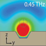
Abstract: We experimentally examine anisotropically etched silicon surfaces for terahertz (THz) plasmonic guided wave applications. Highly doped silicon surfaces are anisotropically etched to form a one dimensional array of sub-wavelength concave pyramidal troughs. The plasmonic waveguides are found to support highly confined guided modes both in transverse and longitudinal directions. The resonant frequencies of the modes can be controlled by adjusting the geometrical parameters of the troughs. The existence of guided modes in plasmonic waveguides is also established through finite-element-based numerical simulations. These waveguides could provide a silicon-based alternative to metallic waveguides for use in future THz devices.Citation:
S. Li, M. M. Jadidi, T. E. Murphy and G. Kumar, "Plasmonic terahertz waveguide based on anisotropically etched silicon substrate", IEEE Trans. Terahertz Sci. Technol. 4(4) 454-458 (2014)
Export: BibTeX | RIS
Manuscript: Li_TTST_4_454_2014.pdf
