Published/Posted: August 29, 2013
Authors: Kumar, G.; Li, S.; Jadidi, M. M.; Murphy, T. E.
DOI: 10.1088/1367-2630/15/8/085031
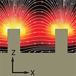
Abstract: We experimentally demonstrate a three-dimensional plasmonic terahertz waveguide by lithographically patterning an array of sub-wavelength pillars on a silicon substrate. Doped silicon can exhibit conductive properties at terahertz frequencies, making it a convenient substitute for conventional metals in plasmonic devices. However, the surface wave solution at a doped silicon surface is usually poorly confined and lossy. Here we demonstrate that by patterning the silicon surface with an array of sub-wavelength pillars, the resulting structure can support a terahertz surface mode that is tightly confined in both transverse directions. Further, we observe that the resonant behavior associated with the surface modes depends on the dimensions of the pillars, and can be tailored through control of the structural parameters. We experimentally fabricated devices with different geometries, and characterized the performance using terahertz time-domain spectroscopy. The resulting waveguide characteristics are confirmed using finite element numerical simulations, and we further show that a simple one-dimensional analytical theory adequately predicts the observed dispersion relation.Citation:
G. Kumar, S. Li, M. M. Jadidi and T. E. Murphy, "Terahertz surface plasmon waveguide based on a one-dimensional array of silicon pillars", New J. Phys. 15(8) 085031 (2013)
Export: BibTeX | RIS
Manuscript: Kumar_NJP_15_085031_2013.pdf